Bipolar Transistor Basics

Bipolar Transistor Basics

In the Diode tutorials we saw that simple diodes are made up from two pieces of semiconductor material, either silicon or germanium to form a simple PN-junction and we also learnt about their properties and characteristics. If we now join together two individual signal diodes back-to-back, this will give us two PN-junctions connected together in series that share a common P or N terminal. The fusion of these two diodes produces a three layer, two junction, three terminal device forming the basis of a Bipolar Junction Transistor, or BJT for short.

Transistors are three terminal active devices made from different semiconductor materials that can act as either an insulator or a conductor by the application of a small signal voltage. The transistor’s ability to change between these two states enables it to have two basic functions: “switching” (digital electronics) or “amplification” (analogue electronics). Then bipolar transistors have the ability to operate within three different regions:

  • 1. Active Region   –   the transistor operates as an amplifier and Ic = β.Ib
  • 2. Saturation   –   the transistor is “fully-ON” operating as a switch and Ic = I(saturation)
  • 3. Cut-off   –   the transistor is “fully-OFF” operating as a switch and Ic = 0

The word Transistor is an acronym, and is a combination of the words Transfer Varistor used to describe their mode of operation way back in their early days of development. There are two basic types of bipolar transistor construction, PNP and NPN, which basically describes the physical arrangement of the P-type and N-type semiconductor materials from which they are made.

The Bipolar Transistor basic construction consists of two PN-junctions producing three connecting terminals with each terminal being given a name to identify it from the other two. These three terminals are known and labelled as the Emitter ( E ), the Base ( B ) and the Collector ( C ) respectively.

Bipolar Transistors are current regulating devices that control the amount of current flowing through them in proportion to the amount of biasing voltage applied to their base terminal acting like a current-controlled switch. The principle of operation of the two transistor types PNP and NPN, is exactly the same the only difference being in their biasing and the polarity of the power supply for each type.

Bipolar Transistor Construction

The construction and circuit symbols for both the PNP and NPN bipolar transistor are given above with the arrow in the circuit symbol always showing the direction of “conventional current flow” between the base terminal and its emitter terminal. The direction of the arrow always points from the positive P-type region to the negative N-type region for both transistor types, exactly the same as for the standard diode symbol.

Bipolar Transistor Configurations

As the Bipolar Transistor is a three terminal device, there are basically three possible ways to connect it within an electronic circuit with one terminal being common to both the input and output. Each method of connection responding differently to its input signal within a circuit as the static characteristics of the transistor vary with each circuit arrangement.

  • 1. Common Base Configuration   –   has Voltage Gain but no Current Gain.
  • 2. Common Emitter Configuration   –   has both Current and Voltage Gain.
  • 3. Common Collector Configuration   –   has Current Gain but no Voltage Gain.

The Common Base (CB) Configuration

As its name suggests, in the Common Base or grounded base configuration, the BASE connection is common to both the input signal AND the output signal with the input signal being applied between the base and the emitter terminals. The corresponding output signal is taken from between the base and the collector terminals as shown with the base terminal grounded or connected to a fixed reference voltage point. The input current flowing into the emitter is quite large as its the sum of both the base current and collector current respectively therefore, the collector current output is less than the emitter current input resulting in a current gain for this type of circuit of “1” (unity) or less, in other words the common base configuration “attenuates” the input signal.

The Common Base Transistor Circuit

This type of amplifier configuration is a non-inverting voltage amplifier circuit, in that the signal voltages Vin and Vout are in-phase. This type of transistor arrangement is not very common due to its unusually high voltage gain characteristics. Its output characteristics represent that of a forward biased diode while the input characteristics represent that of an illuminated photo-diode. Also this type of bipolar transistor configuration has a high ratio of output to input resistance or more importantly “load” resistance (RL) to “input” resistance (Rin) giving it a value of “Resistance Gain”. Then the voltage gain (Av) for a common base configuration is therefore given as:

Common Base Voltage Gain

Where: Ic/Ie is the current gain, alpha (α) and RL/Rin is the resistance gain.

The common base circuit is generally only used in single stage amplifier circuits such as microphone pre-amplifier or radio frequency (Rf) amplifiers due to its very good high frequency response.

The Common Emitter (CE) Configuration

In the Common Emitter or grounded emitter configuration, the input signal is applied between the base, while the output is taken from between the collector and the emitter as shown. This type of configuration is the most commonly used circuit for transistor based amplifiers and which represents the “normal” method of bipolar transistor connection. The common emitter amplifier configuration produces the highest current and power gain of all the three bipolar transistor configurations. This is mainly because the input impedance is LOW as it is connected to a forward-biased PN-junction, while the output impedance is HIGH as it is taken from a reverse-biased PN-junction.

The Common Emitter Amplifier Circuit
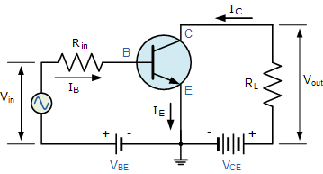
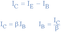
In this type of configuration, the current flowing out of the transistor must be equal to the currents flowing into the transistor as the emitter current is given as Ie = Ic + Ib. Also, as the load resistance (RL) is connected in series with the collector, the current gain of the common emitter transistor configuration is quite large as it is the ratio of Ic/Ib and is given the Greek symbol of Beta, (β). As the emitter current for a common emitter configuration is defined as Ie = Ic + Ib, the ratio of Ic/Ie is called Alpha, given the Greek symbol of α. Note: that the value of Alpha will always be less than unity.

Since the electrical relationship between these three currents, Ib, Ic and Ie is determined by the physical construction of the transistor itself, any small change in the base current (Ib), will result in a much larger change in the collector current (Ic). Then, small changes in current flowing in the base will thus control the current in the emitter-collector circuit. Typically, Beta has a value between 20 and 200 for most general purpose transistors.

By combining the expressions for both Alpha, α and Beta, β the mathematical relationship between these parameters and therefore the current gain of the transistor can be given as:

Where: “Ic” is the current flowing into the collector terminal, “Ib” is the current flowing into the base terminal and “Ie” is the current flowing out of the emitter terminal.

Then to summarise, this type of bipolar transistor configuration has a greater input impedance, current and power gain than that of the common base configuration but its voltage gain is much lower. The common emitter configuration is an inverting amplifier circuit resulting in the output signal being 180o out-of-phase with the input voltage signal.

The Common Collector (CC) Configuration

In the Common Collector or grounded collector configuration, the collector is now common through the supply. The input signal is connected directly to the base, while the output is taken from the emitter load as shown. This type of configuration is commonly known as a Voltage Follower or Emitter Follower circuit. The emitter follower configuration is very useful for impedance matching applications because of the very high input impedance, in the region of hundreds of thousands of Ohms while having a relatively low output impedance.

The Common Collector Transistor Circuit

The common emitter configuration has a current gain approximately equal to the β value of the transistor itself. In the common collector configuration the load resistance is situated in series with the emitter so its current is equal to that of the emitter current. As the emitter current is the combination of the collector AND the base current combined, the load resistance in this type of transistor configuration also has both the collector current and the input current of the base flowing through it. Then the current gain of the circuit is given as:

The Common Collector Current Gain

This type of bipolar transistor configuration is a non-inverting circuit in that the signal voltages of Vin and Vout are in-phase. It has a voltage gain that is always less than “1” (unity). The load resistance of the common collector transistor receives both the base and collector currents giving a large current gain (as with the common emitter configuration) therefore, providing good current amplification with very little voltage gain.

Bipolar Transistor Summary

Then to summarise, the behaviour of the bipolar transistor in each one of the above circuit configurations is very different and produces different circuit characteristics with regards to input impedance, output impedance and gain whether this is voltage gain, current gain or power gain and this is summarised in the table below.

Bipolar Transistor Characteristics

The static characteristics for a Bipolar Transistor can be divided into the following three main groups.

Input Characteristics:-  Common Base  – ΔVEB / ΔIE
 Common Emitter  – ΔVBE / ΔIB
Output Characteristics:-  Common Base  – ΔVC / ΔIC
 Common Emitter  – ΔVC / ΔIC
Transfer Characteristics:-  Common Base  – ΔIC / ΔIE
 Common Emitter  – ΔIC / ΔIB

with the characteristics of the different transistor configurations given in the following table:

Characteristic Common
Base
Common
Emitter
Common
Collector
Input Impedance Low Medium High
Output Impedance Very High High Low
Phase Angle 0o 180o 0o
Voltage Gain High Medium Low
Current Gain Low Medium High
Power Gain Low Very High Medium

In the next tutorial about Bipolar Transistors, we will look at the NPN Transistor in more detail when used in the common emitter configuration as an amplifier as this is the most widely used configuration due to its flexibility and high gain. We will also plot the output characteristics curves commonly associated with amplifier circuits as a function of the collector current to the base current.
The NPN Transistor

The NPN Transistor

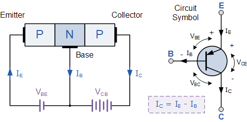
In the previous tutorial we saw that the standard Bipolar Transistor or BJT, comes in two basic forms. An NPN (Negative-Positive-Negative) type and a PNP (Positive-Negative-Positive) type, with the most commonly used transistor type being the NPN Transistor. We also learnt that the transistor junctions can be biased in one of three different ways – Common Base, Common Emitter and Common Collector. In this tutorial we will look more closely at the “Common Emitter” configuration using NPN Transistors with an example of the construction of a NPN transistor along with the transistors current flow characteristics is given below.

An NPN Transistor Configuration

(Note: Arrow defines the emitter and conventional current flow, “out” for an NPN transistor.)

The construction and terminal voltages for an NPN transistor are shown above. The voltage between the Base and Emitter ( VBE ), is positive at the Base and negative at the Emitter because for an NPN transistor, the Base terminal is always positive with respect to the Emitter. Also the Collector supply voltage is positive with respect to the Emitter ( VCE ). So for an NPN transistor to conduct the Collector is always more positive with respect to both the Base and the Emitter.

Then the voltage sources are connected to an NPN transistor as shown. The Collector is connected to the supply voltage VCC via the load resistor, RL which also acts to limit the maximum current flowing through the device. The Base supply voltage VB is connected to the Base resistor RB, which again is used to limit the maximum Base current.

We know that the transistor is a “current” operated device (Beta model) and that a large current ( Ic ) flows freely through the device between the collector and the emitter terminals when the transistor is switched “fully-ON”. However, this only happens when a small biasing current ( Ib ) is flowing into the base terminal of the transistor at the same time thus allowing the Base to act as a sort of current control input.

The transistor current in an NPN transistor is the ratio of these two currents ( Ic/Ib ), called the DC Current Gain of the device and is given the symbol of hfe or nowadays Beta, ( β ). The value of β can be large up to 200 for standard transistors, and it is this large ratio between Ic and Ib that makes the NPN transistor a useful amplifying device when used in its active region as Ib provides the input and Ic provides the output. Note that Beta has no units as it is a ratio.

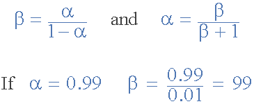
Also, the current gain of the transistor from the Collector terminal to the Emitter terminal, Ic/Ie, is called Alpha, ( α ), and is a function of the transistor itself (electrons diffusing across the junction). As the emitter current Ie is the product of a very small base current plus a very large collector current, the value of alpha α, is very close to unity, and for a typical low-power signal transistor this value ranges from about 0.950 to 0.999

α and β Relationship in a NPN Transistor

By combining the two parameters α and β we can produce two mathematical expressions that gives the relationship between the different currents flowing in the transistor.

The values of Beta vary from about 20 for high current power transistors to well over 1000 for high frequency low power type bipolar transistors. The value of Beta for most standard NPN transistors can be found in the manufactures datasheets but generally range between 50 – 200.

The equation above for Beta can also be re-arranged to make Ic as the subject, and with a zero base current ( Ib = 0 ) the resultant collector current Ic will also be zero, ( β x 0 ). Also when the base current is high the corresponding collector current will also be high resulting in the base current controlling the collector current. One of the most important properties of the Bipolar Junction Transistor is that a small base current can control a much larger collector current. Consider the following example.

Example No1

An NPN Transistor has a DC current gain, (Beta) value of 200. Calculate the base current Ib required to switch a resistive load of 4mA.

Therefore, β = 200, Ic = 4mA and Ib = 20µA.

One other point to remember about NPN Transistors. The collector voltage, ( Vc ) must be greater and positive with respect to the emitter voltage, ( Ve ) to allow current to flow through the transistor between the collector-emitter junctions. Also, there is a voltage drop between the Base and the Emitter terminal of about 0.7v (one diode volt drop) for silicon devices as the input characteristics of an NPN Transistor are of a forward biased diode. Then the base voltage, ( Vbe ) of a NPN transistor must be greater than this 0.7V otherwise the transistor will not conduct with the base current given as.

Where:   Ib is the base current, Vb is the base bias voltage, Vbe is the base-emitter volt drop (0.7v) and Rb is the base input resistor. Increasing Ib, Vbe slowly increases to 0.7V but Ic rises exponentially.

Example No2

An NPN Transistor has a DC base bias voltage, Vb of 10v and an input base resistor, Rb of 100kΩ. What will be the value of the base current into the transistor

Therefore, Ib = 93µA.

The Common Emitter Configuration.

As well as being used as a semiconductor switch to turn load currents “ON” or “OFF” by controlling the Base signal to the transistor in ether its saturation or cut-off regions, NPN Transistors can also be used in its active region to produce a circuit which will amplify any small AC signal applied to its Base terminal with the Emitter grounded. If a suitable DC “biasing” voltage is firstly applied to the transistors Base terminal thus allowing it to always operate within its linear active region, an inverting amplifier circuit called a single stage common emitter amplifier is produced.

One such Common Emitter Amplifier configuration of an NPN transistor is called a Class A Amplifier. A “Class A Amplifier” operation is one where the transistors Base terminal is biased in such a way as to forward bias the Base-emitter junction. The result is that the transistor is always operating halfway between its cut-off and saturation regions, thereby allowing the transistor amplifier to accurately reproduce the positive and negative halves of any AC input signal superimposed upon this DC biasing voltage. Without this “Bias Voltage” only one half of the input waveform would be amplified. This common emitter amplifier configuration using an NPN transistor has many applications but is commonly used in audio circuits such as pre-amplifier and power amplifier stages.

With reference to the common emitter configuration shown below, a family of curves known as the Output Characteristics Curves, relates the output collector current, (Ic) to the collector voltage, (Vce) when different values of Base current, (Ib) are applied to the transistor for transistors with the same β value. A DC “Load Line” can also be drawn onto the output characteristics curves to show all the possible operating points when different values of base current are applied. It is necessary to set the initial value of Vce correctly to allow the output voltage to vary both up and down when amplifying AC input signals and this is called setting the operating point or Quiescent Point, Q-point for short and this is shown below.

Single Stage Common Emitter Amplifier Circuit

Output Characteristics Curves of a Typical Bipolar Transistor

The most important factor to notice is the effect of Vce upon the collector current Ic when Vce is greater than about 1.0 volts. We can see that Ic is largely unaffected by changes in Vce above this value and instead it is almost entirely controlled by the base current, Ib. When this happens we can say then that the output circuit represents that of a “Constant Current Source”. It can also be seen from the common emitter circuit above that the emitter current Ie is the sum of the collector current, Ic and the base current, Ib, added together so we can also say that Ie = Ic + Ib for the common emitter (CE) configuration.

By using the output characteristics curves in our example above and also Ohm´s Law, the current flowing through the load resistor, (RL), is equal to the collector current, Ic entering the transistor which inturn corresponds to the supply voltage, (Vcc) minus the voltage drop between the collector and the emitter terminals, (Vce) and is given as:

Also, a straight line representing the Dynamic Load Line of the transistor can be drawn directly onto the graph of curves above from the point of “Saturation” ( A ) when Vce = 0 to the point of “Cut-off” ( B ) when Ic = 0 thus giving us the “Operating” or Q-point of the transistor. These two points are joined together by a straight line and any position along this straight line represents the “Active Region” of the transistor. The actual position of the load line on the characteristics curves can be calculated as follows:

Then, the collector or output characteristics curves for Common Emitter NPN Transistors can be used to predict the Collector current, Ic, when given Vce and the Base current, Ib. A Load Line can also be constructed onto the curves to determine a suitable Operating or Q-point which can be set by adjustment of the base current. The slope of this load line is equal to the reciprocal of the load resistance which is given as: -1/RL

Then we can define a NPN Transistor as being normally “OFF” but a small input current and a small positive voltage at its Base (B) relative to its Emitter (E) will turn it “ON” allowing a much large Collector-Emitter current to flow. NPN transistors conduct when Vc is much greater than Ve.

In the next tutorial about Bipolar Transistors, we will look at the opposite or complementary form of the NPN Transistor called the PNP Transistor and show that the PNP Transistor has very similar characteristics to their NPN transistor except that the polarities (or biasing) of the current and voltage directions are reversed.

The PNP Transistor

The PNP Transistor

The PNP Transistor is the exact opposite to the NPN Transistor device we looked at in the previous tutorial. Basically, in this type of transistor construction the two diodes are reversed with respect to the NPN type giving a Positive-Negative-Positive configuration, with the arrow which also defines the Emitter terminal this time pointing inwards in the transistor symbol.

Also, all the polarities for a PNP transistor are reversed which means that it “sinks” current into its Base as opposed to the NPN transistor which “sources” current through its Base. The main difference between the two types of transistors is that holes are the more important carriers for PNP transistors, whereas electrons are the important carriers for NPN transistors. Then, PNP transistors use a small base current and a negative base voltage to control a much larger emitter-collector current. In other words for a PNP transistor, the Emitter is more positive with respect to the Base and also with respect to the Collector.

The construction of a “PNP transistor” consists of two P-type semiconductor materials either side of an N-type material as shown below.

A PNP Transistor Configuration

(Note: Arrow defines the emitter and conventional current flow, “in” for a PNP transistor.)
The construction and terminal voltages for an NPN transistor are shown above. The PNP Transistor has very similar characteristics to their NPN bipolar cousins, except that the polarities (or biasing) of the current and voltage directions are reversed for any one of the possible three configurations looked at in the first tutorial, Common Base, Common Emitter and Common Collector.

The voltage between the Base and Emitter ( VBE ), is now negative at the Base and positive at the Emitter because for a PNP transistor, the Base terminal is always biased negative with respect to the Emitter. Also the Emitter supply voltage is positive with respect to the Collector ( VCE ). So for a PNP transistor to conduct the Emitter is always more positive with respect to both the Base and the Collector.

The voltage sources are connected to a PNP transistor are as shown. This time the Emitter is connected to the supply voltage VCC with the load resistor, RL which limits the maximum current flowing through the device connected to the Collector terminal. The Base voltage VB which is biased negative with respect to the Emitter and is connected to the Base resistor RB, which again is used to limit the maximum Base current.

To cause the Base current to flow in a PNP transistor the Base needs to be more negative than the Emitter (current must leave the base) by approx 0.7 volts for a silicon device or 0.3 volts for a germanium device with the formulas used to calculate the Base resistor, Base current or Collector current are the same as those used for an equivalent NPN transistor and is given as.

Generally, the PNP transistor can replace NPN transistors in most electronic circuits, the only difference is the polarities of the voltages, and the directions of the current flow. PNP transistors can also be used as switching devices and an example of a PNP transistor switch is shown below.

A PNP Transistor Circuit

The Output Characteristics Curves for a PNP transistor look very similar to those for an equivalent NPN transistor except that they are rotated by 180o to take account of the reverse polarity voltages and currents, (the currents flowing out of the Base and Collector in a PNP transistor are negative). The same dynamic load line can be drawn onto the I-V curves to find the PNP transistors operating points.

Transistor Matching

You may think what is the point of having a PNP Transistor, when there are plenty of NPN Transistors available that can be used as an amplifier or solid-state switch?. Well, having two different types of transistors “PNP” and “NPN”, can be a great advantage when designing amplifier circuits such as the Class B Amplifier which uses “Complementary” or “Matched Pair” transistors in its output stage or in reversible H-Bridge motor control circuits were we want to control the flow of current evenly in both directions.

A pair of corresponding NPN and PNP transistors with near identical characteristics to each other are called Complementary Transistors for example, a TIP3055 (NPN transistor) and the TIP2955 (PNP transistor) are good examples of complementary or matched pair silicon power transistors. They both have a DC current gain, Beta, ( Ic/Ib ) matched to within 10% and high Collector current of about 15A making them ideal for general motor control or robotic applications.

Also, class B amplifiers use complementary NPN and PNP in their power output stage design. The NPN transistor conducts for only the positive half of the signal while the PNP transistor conducts for negative half of the signal. This allows the amplifier to drive the required power through the load loudspeaker in both directions at the stated nominal impedance and power resulting in an output current which is likely to be in the order of several amps shared evenly between the two complementary transistors.

Identifying the PNP Transistor

We saw in the first tutorial of this transistors section, that transistors are basically made up of two Diodes connected together back-to-back. We can use this analogy to determine whether a transistor is of the PNP type or NPN type by testing its Resistance between the three different leads, Emitter, Base and Collector. By testing each pair of transistor leads in both directions with a multimeter will result in six tests in total with the expected resistance values in Ohm’s given below.

  • 1. Emitter-Base Terminals – The Emitter to Base should act like a normal diode and conduct one way only.
  • 2. Collector-Base Terminals – The Collector-Base junction should act like a normal diode and conduct one way only.
  • 3. Emitter-Collector Terminals – The Emitter-Collector should not conduct in either direction.

Transistor resistance values for a PNP transistor and a NPN transistor

Between Transistor Terminals PNP NPN
Collector Emitter RHIGH RHIGH
Collector Base RLOW RHIGH
Emitter Collector RHIGH RHIGH
Emitter Base RLOW RHIGH
Base Collector RHIGH RLOW
Base Emitter RHIGH RLOW


Then we can define a PNP Transistor as being normally “OFF” but a small output current and negative voltage at its Base (B) relative to its Emitter (E) will turn it “ON” allowing a much large Emitter-Collector current to flow. PNP transistors conduct when Ve is much greater than Vc.

In the next tutorial about Bipolar Transistors instead of using the transistor as an amplifying device, we will look at the operation of the transistor in its saturation and cut-off regions when used as a solid-state switch. Bipolar transistor switches are used in many applications to switch a DC current “ON” or “OFF” such as LED’s which require only a few milliamps at low DC voltages, or relays which require higher currents at higher voltages.

The Transistor as a Switch

When used as an AC signal amplifier, the transistors Base biasing voltage is applied in such a way that it always operates within its “active” region, that is the linear part of the output characteristics curves are used. However, both the NPN & PNP type bipolar transistors can be made to operate as “ON/OFF” type solid state switches by biasing the transistors base differently to that of a signal amplifier. Solid state switches are one of the main applications for the use of transistors, and transistor switches can be used for controlling high power devices such as motors, solenoids or lamps, but they can also used in digital electronics and logic gate circuits.

If the circuit uses the Bipolar Transistor as a Switch, then the biasing of the transistor, either NPN or PNP is arranged to operate the transistor at both sides of the ” I-V ” characteristics curves we have seen previously. The areas of operation for a transistor switch are known as the Saturation Region and the Cut-off Region. This means then that we can ignore the operating Q-point biasing and voltage divider circuitry required for amplification, and use the transistor as a switch by driving it back and forth between its “fully-OFF” (cut-off) and “fully-ON” (saturation) regions as shown below.

1. Cut-off Region

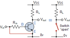
Here the operating conditions of the transistor are zero input base current ( IB ), zero output collector current ( IC ) and maximum collector voltage ( VCE ) which results in a large depletion layer and no current flowing through the device. Therefore the transistor is switched “Fully-OFF”.

Cut-off Characteristics


  • The input and Base are grounded (0v)
  • Base-Emitter voltage VBE < 0.7v
  • Base-Emitter junction is reverse biased
  • Base-Collector junction is reverse biased
  • Transistor is “fully-OFF” (Cut-off region)
  • No Collector current flows ( IC = 0 )
  • VOUT = VCE = VCC = “1”
  • Transistor operates as an “open switch”

Then we can define the “cut-off region” or “OFF mode” when using a bipolar transistor as a switch as being, both junctions reverse biased, VB < 0.7v and IC = 0. For a PNP transistor, the Emitter potential must be negative with respect to the Base.

2. Saturation Region

Here the transistor will be biased so that the maximum amount of base current is applied, resulting in maximum collector current resulting in the minimum collector emitter voltage drop which results in the depletion layer being as small as possible and maximum current flowing through the transistor. Therefore the transistor is switched “Fully-ON”.

Saturation Characteristics

  • The input and Base are connected to VCC
  • Base-Emitter voltage VBE > 0.7v
  • Base-Emitter junction is forward biased
  • Base-Collector junction is forward biased
  • Transistor is “fully-ON” (saturation region)
  • Max Collector current flows (IC = Vcc/RL)
  • VCE = 0 (ideal saturation)
  • VOUT = VCE = “0”
  • Transistor operates as a “closed switch”

Then we can define the “saturation region” or “ON mode” when using a bipolar transistor as a switch as being, both junctions forward biased, VB > 0.7v and IC = Maximum. For a PNP transistor, the Emitter potential must be positive with respect to the Base.

Then the transistor operates as a “single-pole single-throw” (SPST) solid state switch. With a zero signal applied to the Base of the transistor it turns “OFF” acting like an open switch and zero collector current flows. With a positive signal applied to the Base of the transistor it turns “ON” acting like a closed switch and maximum circuit current flows through the device.

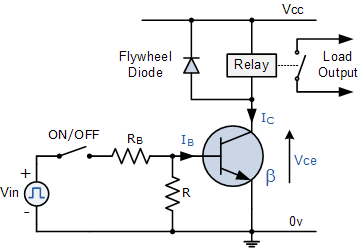
An example of an NPN Transistor as a switch being used to operate a relay is given below. With inductive loads such as relays or solenoids a flywheel diode is placed across the load to dissipate the back EMF generated by the inductive load when the transistor switches “OFF” and so protect the transistor from damage. If the load is of a very high current or voltage nature, such as motors, heaters etc, then the load current can be controlled via a suitable relay as shown.

Saturation Transistor
  • The input and Base are connected to VCC
  • Base-Emitter voltage VBE > 0.7v
  • Base-Emitter junction is forward biased
  • Base-Collector junction is forward biased
  • Transistor is “fully-ON” (saturation region)
  • Max Collector current flows (IC = Vcc/RL)
  • VCE = 0 (ideal saturation)
  • VOUT = VCE = “0”
  • Transistor operates as a “closed switch”

Basic NPN Transistor Switching Circuit

The circuit resembles that of the Common Emitter circuit we looked at in the previous tutorials. The difference this time is that to operate the transistor as a switch the transistor needs to be turned either fully “OFF” (cut-off) or fully “ON” (saturated). An ideal transistor switch would have infinite circuit resistance between the Collector and Emitter when turned “fully-OFF” resulting in zero current flowing through it and zero resistance between the Collector and Emitter when turned “fully-ON”, resulting in maximum current flow. In practice when the transistor is turned “OFF”, small leakage currents flow through the transistor and when fully “ON” the device has a low resistance value causing a small saturation voltage ( VCE ) across it. Even though the transistor is not a perfect switch, in both the cut-off and saturation regions the power dissipated by the transistor is at its minimum.

In order for the Base current to flow, the Base input terminal must be made more positive than the Emitter by increasing it above the 0.7 volts needed for a silicon device. By varying this Base-Emitter voltage VBE,  the Base current is also altered and which in turn controls the amount of Collector current flowing through the transistor as previously discussed. When maximum Collector current flows the transistor is said to be Saturated. The value of the Base resistor determines how much input voltage is required and corresponding Base current to switch the transistor fully “ON”.

Example No1

Using the transistor values from the previous tutorials of:  β = 200, Ic = 4mA and Ib = 20uA, find the value of the Base resistor (Rb) required to switch the load fully “ON” when the input terminal voltage exceeds 2.5v.

The next lowest preferred value is: 82kΩ, this guarantees the transistor switch is always saturated.

Example No2

Again using the same values, find the minimum Base current required to turn the transistor “fully-ON” (saturated) for a load that requires 200mA of current when the input voltage is increased to 5.0V. Also calculate the new value of Rb.

transistor Base current:

transistor Base resistance:

Transistor switches are used for a wide variety of applications such as interfacing large current or high voltage devices like motors, relays or lamps to low voltage digital logic IC’s or gates like AND gates or OR gates. Here, the output from a digital logic gate is only +5v but the device to be controlled may require a 12 or even 24 volts supply. Or the load such as a DC Motor may need to have its speed controlled using a series of pulses (Pulse Width Modulation). transistor switches will allow us to do this faster and more easily than with conventional mechanical switches.

PNP Transistor Switch

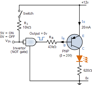
We can also use PNP transistors as switches, the difference this time is that the load is connected to ground (0v) and the PNP transistor switches power to it. To turn the PNP transistor as a switch “ON” the Base terminal is connected to ground or zero volts (LOW) as shown.

The equations for calculating the Base resistance, Collector current and voltages are exactly the same as for the previous NPN transistor switch. The difference this time is that we are switching power with a PNP transistor (sourcing current) instead of switching ground with an NPN transistor (sinking current).